Electron Diffraction
Experimental Apparatus
3.1 Optical Diffraction
The optical diffraction apparatus is shown in Figure 3.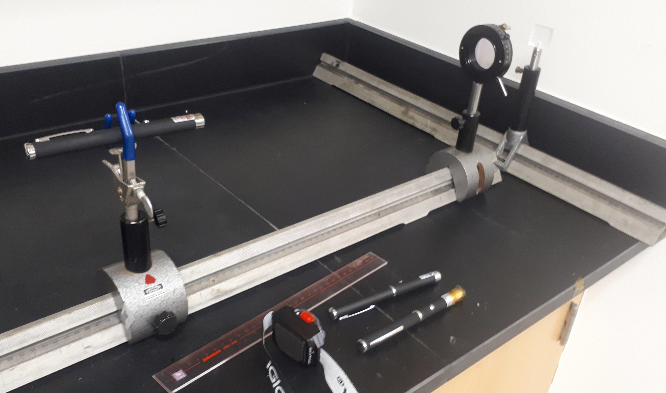
Figure 3: Apparatus used for optical diffraction. The claw holds the diode laser. Downstream from the laser is the diffraction grating, and behind that is the rail and alignment tool used for position measurements.
The light source is a diode laser (i.e. laser pointer). There is a huge wealth of physics and engineering that explain why a laser diode can emit light. It basically comes down to electron-hole pairs recombining in a p-n doped semiconductor. If you’re interested, check out Wikipedia for more details. For a long time, experimentalists were limited to red helium-neon (HeNe). And then diode lasers become more widely available and they were almost exclusively red for a long time. And now there are so many colours of laser pointer for like 10 CAD! The wavelength of each laser, and its uncertainty, is written on the head of the diode laser.
The light from the diode is diffracted using a diffraction grating. A diffraction grating is basically the double-slit setup on steroids. Common, cheap gratings typically have hundreds of lines (slits) per millimeter! Gratings with a high number of lines per millimeter result in larger DIFFERENCES in deflection angle for DIFFERENT wavelengths, and so are useful in separating incoming light into its various colours. Take a good look at Equation (1) to check if that last sentence was true.
3.2 Electron Diffraction
The electron diffraction apparatus is shown in Figure 4.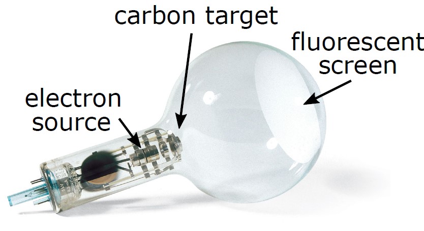
Figure 4: Apparatus used for electron diffraction. The power supply is not shown.
The electrons in this experiment are the result of a heated tungsten filament due to a process called thermionic emission. The electrons are accelerated by an applied electric field. The kinetic energy gained by the electrons is equal to the applied potential multiplied by the electric charge:
(3) 
where  is the charge of the electron.
Lattice spacing in crystals are much smaller than any grating that could be manufactured. Assuming carbon forms a simple cubic system, we can estimate its lattice structure. 12 grams of carbon contain 6×10²³ atoms (thanks, Avogadro!). The density of carbon is about 2 grams/cm , so 1 cm contains 1023 atoms, and adjacent carbon atoms will be
 ![\sqrt[3]{10}](https://ecampusontario.pressbooks.pub/app/uploads/quicklatex/quicklatex.com-5d6adca42b922b148e324ed592213326_l3.png "Rendered by QuickLaTeX.com") , or a little over 2 angstroms apart. What will the diffraction angle be using a carbon lattice as a grating for our 3 to 5 kV electrons?
, or a little over 2 angstroms apart. What will the diffraction angle be using a carbon lattice as a grating for our 3 to 5 kV electrons?
If the carbon lattice was uniformly arranged, we could expect to see a ‘cross’ diffraction pattern, as shown in Figure 5(a). The lattice of our carbon sample is randomly arranged, creating a ring pattern, as in Figure 5(b). Variation of the anode voltage will change the diameter of the ring, in accord with de Broglie’s suggestions that wavelength and momentum are related.
The electrons are detected by a fluorescent coating that glows when bombarded by electrons. The distance between the graphite/carbon sample and the fluorescent screen is 13.5 cm.

Figure 5: (a) The diffraction pattern from a uniformly arranged lattice. (b) The diffraction pattern from a randomly arranged lattice