6.3 – Operational Amplifiers – Basics
Operational Amplifiers - Basics
An operational amplifier is, in essence, a multi-stage high gain amplifier treated as a single entity. Normally, op-amps have a differential input and a single-ended output. In other words, one input produces an inverted output signal, and the other input produces a noninverted output signal. Often, the op-amp is driven from a bipolar power supply (i.e., two supplies, one positive and one negative). Just about any sort of active amplifying device may be used for the individual stages. Op amps can be made entirely from vacuum tubes or discrete bipolar transistors. The advances in semiconductor manufacture in the late 1960s and early 1970s eventually made it possible to miniaturize the required components and place the whole affair on a single silicon chip (hence the term, integrated circuit). Through common use, this is what is generally meant by the term op amp today.
As seen in Fig. 6.3.1, a typical op amp has at least five distinct connections; an inverting input (labeled “−”), a noninverting input (labeled “+”), an output, and positive and negative power supply inputs. These power supply connections are sometimes referred to as supply rails. Note that a ground connection is not directly given. Rather, a ground connection is implied through the other connections. This symbol and its associated connections are typical, but by no means absolute. There are a wide variety of devices available to the designer that offer such features as differential outputs or unipolar power supply operation. In any case, some form of triangle will be used for the schematic symbol.
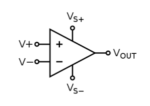
Figure 6.3.1 - Schematic symbol for op-amp
The operational amplifier is arguably the most useful single device in analog electronic circuitry. With only a handful of external components, it can be made to perform a wide variety of analog signal processing tasks. It is also quite affordable, most general-purpose amplifiers selling for under a dollar apiece. Modern designs have been engineered with durability in mind as well: several “op-amps” are manufactured that can sustain direct short-circuits on their outputs without damage.
Where might you find op amp circuits? In a word, anywhere. They're probably in use in your home stereo or TV where they help capture incoming signals, in electronic musical instruments where they can be used to create and modify tones, in a camera in conjunction with a light metering system, or in medical instruments where they might be used along with various bio-sensing devices.
Block Diagram of an Op-amp
At this point you may be asking yourself, “what's inside of the op amp?” The generic op amp consists of three main functional stages. A real op amp may contain more than three distinct stages, but can be reduced to this level for analysis. A generalized discrete representation is given in Figure 6.3.2. Since the op amp requires a differential input scheme, the first stage is most often a differential amplifier. As seen here, [latex]Q_1[/latex] and [latex]Q_2[/latex] comprise a PNP-based differential amplifier. The output of one collector ([latex]Q_2[/latex] here) is then fed to a high-gain second stage. This stage usually includes a lag network capacitor that plays a major roll in setting the op amp's AC characteristics. [latex]Q_3[/latex] makes up the second stage in the example. It is set in a common emitter configuration for both current and voltage gain. The aforementioned lag capacitor is positioned across [latex]Q_3[/latex]'s base collector junction in order to take advantage of the Miller effect. The third and final section is a class B or class AB follower for the most effective load drive. [latex]Q_4[/latex] and [latex]Q_5[/latex] make up the final stage. The twin diodes compensate for the [latex]Q_4[/latex] and [latex]Q_5[/latex] VBE drops, and produce a trickle bias current that minimizes distortion. This is a relatively standard class AB stage. Note that the entire circuit is direct-coupled. There are no lead networks, and thus the op amp can amplify down to zero hertz (DC). There are
many possible changes that may be seen in a real world circuit, including the use of Darlington pairs or FETs for the differential amplifier, multiple high gain stages, and output current limiting for the class B section.
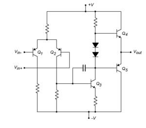
Figure 6.3.2 - Schematic for a general op-amp
Properties of Operational Amplifiers
Operational Amplifiers on their own have a very high open loop DC gain and by applying some form of Negative Feedback we can produce an operational amplifier circuit that has a very precise gain characteristic that is dependent only on the feedback used.
An operational amplifier only responds to the difference between the voltages on its two input terminals, known commonly as the “Differential Input Voltage” and not to their common potential. Then if the same voltage potential is applied to both terminals the resultant output will be zero. An Operational Amplifiers gain is commonly known as the Open Loop Differential Gain, and is given the symbol ([latex]A_0[/latex]).
Op-amp Parameters
- The input resistance, [latex]\text{}R_{in}[/latex], is typically large, on the order of [latex]1 MΩ[/latex].
- The output resistance, [latex]R_{out}[/latex], is small, usually less than [latex]100 Ω[/latex].
- The voltage gain, [latex]G[/latex], is large, exceeding [latex]10^5[/latex]
The large gain catches the eye; it suggests that an op-amp could turn a [latex]1 \text{ mV}[/latex] input signal into a [latex]100 \text{ V}[/latex] one. If you were to build such a circuit—attaching a voltage source to node a, attaching node b to the reference, and looking at the output—you would be disappointed. In dealing with electronic components, you cannot forget the unrepresented but needed power supply.
Unmodeled limitations imposed by power supplies: It is impossible for electronic components to yield voltages that exceed those provided by the power supply or for them to yield currents
that exceed the power supply’s rating. Typical power supply voltages required for op-amp circuits are [latex]\pm 15 \text{ V}[/latex]. Attaching the [latex]1 \text{ mv}[/latex] signal not only would fail to produce a [latex]100 \text{ V}[/latex] signal, the resulting waveform would be severely distorted. While adesirable outcome if you are a rock & roll aficionado, high-quality stereos should not distort signals.
Another consideration in designing circuits with op-amps is that these element values are typical: Careful control of the gain can only be obtained by choosing a circuit so that its element values dictate the resulting gain, which must be smaller than that provided by the op-amp.
Watch
The following video provides an overview of op-amps
![]() To learn how to access the transcript for this video, see "YouTube transcript instructions (opens a new window)"
To learn how to access the transcript for this video, see "YouTube transcript instructions (opens a new window)"
Attributions
Unless otherwise noted, the content of this chapter is adapted from Introduction to Operational Amplifiers (Op-amps) by All About Circuits and is under a Design Science License
Portions of this section were adapted from
- Operational Amplifiers & Linear Integrated Circuits: Theory and Application - 3e by James Fior is licensed under CC BY 4.0
- Fundamentals of Electrical Engineering I by Don H. Johnson is licensed under CC BY 1.0
