6.2 – Amplifiers
Amplifiers
Amplifiers are able to take in small-power signals and output signals of much greater power. The Law of Conservation of Energy states that energy can neither be created nor destroyed. If this Law is true, then it is impossible to build a device capable of taking a small amount of energy and magically transforming it into a large amount of energy. The key to understanding how amplifiers can exist without violating the Law of Conservation of Energy lies in the behavior of active devices.

Because active devices have the ability to control a large amount of electrical power with a small amount of electrical power, they may be arranged in circuit so as to duplicate the form of the input signal power from a larger amount of power supplied by an external power source. The result is a device that appears to magically magnify the power of a small electrical signal (usually an AC voltage waveform) into an identically-shaped waveform of larger magnitude.
The Law of Conservation of Energy is not violated because the additional power is supplied by an external source, usually a DC battery or equivalent. The amplifier neither creates nor destroys energy, but merely reshapes it into the waveform desired as shown in the figure below.
Classifying Amplifiers
Although there are several different types of amplifiers, we will focus on a few of the more common ones:
1. Bipolar junction transistor (BJTs)
A bipolar transistor consists of a three-layer “sandwich” of doped (extrinsic) semiconductor materials, (a and c) either P-N-P or N-P-N (b and c ). Each layer forming the transistor has a specific name, and each layer is provided with a wire contact for connection to a circuit. The schematic symbols are shown in the figure (a) and (c).

Figure 6.2.2 – BJT transistor: (a) PNP schematic symbol, (b) layout, (c) NPN schematic symbol and (d) layout
2. Junction gate field-effect transistor (JFET)
In a junction field-effect transistor or JFET, the controlled current passes from source to drain, or from drain to source as the case may be. The controlling voltage is applied between the gate and the source. Note how the current does not have to cross through a PN junction on its way between the source and drain; the path (called a channel) is an uninterrupted block of semiconductor material.
As shown in Figure 6.2.3, this channel is an N-type semiconductor.
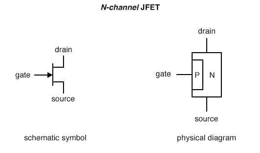
Figure 6.2.3 – Example schematic symbol and diagram of an N-channel JFET
Generally, N-channel JFETs are more commonly used than P-channel (Figure 6.2.4). The only practical difference between N- and P-channel JFETs you need to concern yourself with now is biasing of the PN junction formed between the gate material and the channel. With no voltage applied between the gate and the source, the channel is a wide-open path for current to flow. However, if a voltage is applied between the gate and source of such polarity that it reverse-biases the PN junction, the flow between source and drain connections becomes limited or regulated, just as it was for bipolar transistors with a set amount of base current.
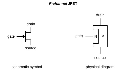
Figure 6.2.4 – schematic symbol and diagram of an P-channel JFET
Both BJTs and JFETs have an output classification based on how the signal is amplified. Although there are several different classes, there are three common output classifications of these amplifiers that we will discuss: Class A, Class B and Class C.
Class A
Class A amplifiers have identical input and output signal configurations. The signal magnitude will change according to the gain characteristics of the transistor.
Advantages: provides better high frequency and feedback loop stability, it is easy to construct with single-device components and has minimum parts count.
Disadvantages: introduces high power loss, provides distortion and noise due to high linearity.
Class B
These are considered the most useful of the three discussed amplifiers since it can be used in a “push-pull” mode and is considered more efficient than a Class A amplifier. Class B amplifiers are created using two active devices which conduct half of the actual cycle i.e. 180 degrees of the cycle. Therefore, the two devices combine to provided the whole current drive for the load.
These amplifiers use one NPN and one PNP transistor that have same in input signal but opposite in phase. This results in one transistor only amplifying one half of the input wave for cycle while the other transistor amplifies the other half.
Advantages: more efficient than Class A amps (up to 78% as opposed to 25-30% for Class A amps) and provides a low heat sink space as heat dissipation is minimized.
Disadvantages: Crossover distortion (this is a big limitation). As the two resistors are responsible for creating one half of the wave cycle, each half of the sinusoidal wave needs to be combined and joined across the output. There is a mismatch (crossover) in the region where the two halves are combined.
Class C
Class C amplifiers have a signal output at a 180 degree difference from Class B amplifier. If a sine wave is the input signal, the positive portion of the waveform is in the cutoff region while the negative portion of the sine wave is amplified at the output.
Advantages: more efficient than Class A and B amplifiers
Disadvantages: large amount of distortion. Due to this, Class C amplifiers are rarely found in biomedical equipment.
3. MOS Field Effect Transistors (MOSFETs)
MOSFET is an acronym for Metallic-Oxide-Semiconductor Field Effect Transistor. A MOSFET is fabricated differently and operates differently than a JFET but it does have some similarities. There are two classes of MOSFETs. There is depletion mode and there is enhancement mode. Each class is available as n- or a p-channel (see Figure 6.2., giving a total of four types of MOSFETs. Depletion mode comes in an N or a P and an enhancement mode comes in an N or a P. Therefore, we have four different types of MOSFETs.

Figure 6.2.5 – schematic symbol of an N and P-channel MOSFET. D = drain, S = source, G = ground
Depletion Mode
Note, there is a continuous channel of n-type material between the source and the drain. A voltage placed across the source and drain would induce current flow. The channel acts like a resistor which is very similar to a JFET. Alternatively, negative voltage will reduce current. It will tend to increase the resistance of the n-type channel and that would reduce current.
The gate is connected to aluminum which is insulated from the channel by a thin layer of silicone dioxide. This is where MOSFETs differ greatly from a FET is we have actual metal here. This metal is aluminum. The aluminum is insulated from the channel by a piece of silicon dioxide. This setup provides no electrical connection between the gate and the n-type material because there is an insulator between them, but you will be able to induce an electronic field through the material. There is no connection between the gate and the source and drain.
The three layers led to the device name hence we have Metallic, Oxide and Semiconductors.
There is also a p-type depletion MOSFET. This is the same as N except for reversal of the material. Again, the same thing except that materials have been reversed.
Enhancement Mode
In Enhancement-mode MOSFETS, the source and drain terminals connect to heavily doped n-type silicon in an n-channel enhancement-mode MOSFET. The area between the source and the drain is lightly doped p-type material. There is no continuous channel between the source and the drain like we had with JFETs and with the depletion-mode. Remember, this is enhancement-mode, this is a major difference right here.
A proper polarity gate voltage must be applied for current flow. A gate voltage will be needed to get current flow. A broken line in the schematic symbol indicates that there is no continuous path from source to drain. When you look at the schematic symbol for an enhanced-mode (e-mode) MOSFET you’ll notice that usually there is continuous line here as we did with FETs and the depletion-mode. For the e-mode MOSFET, it is broken and is broken because it is not a continuous channel.
Attributions
Unless otherwise noted, the content of this chapter is adapted from Amplifiers, Introduction to Bipolar Junction Transistors (BJT), Introduction to Junction Field-effect Transistors (JFET) and MOSFETS – MOS Field Effect Transistors by All About Circuits and is under a Design Science License
- Figure 6.2.1 – Amplifier Icon by Mohamed Mb courtesy of the Noun Project is licensed under CC BY 3.0
- Figure 6.2.5 – MOSFETS by Jaanus.kalde courtesy of Wikimedia Commons. Dedicated to public domain through CC0 license
